Small Signal Animation

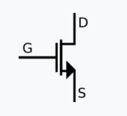
Below is a brief visual explanation of how small signal analysis works for MOSFETs intuitively, assuming some basic understanding of what MOSFETs do.
Gate Voltage on MOSFET
First, understand that applying a larger gate to source voltage (or source to gate, in a PMOS) to a MOSFET will cause more minority carriers to be drawn through the electric field of the gate to the channel connecting the gate and drain.
Of course, the actual current across the MOSFET from source to drain is dependent on the voltage from drain to source (or source to drain in a PMOS, but from this point forward assume an NMOS for simplicity).
Intuitively, it doesn't matter how "open" the channel across the MOSFET is if there is no voltage drop across it for current to flow.
Linear and Saturation Region
With no voltage from drain to source, the MOSFET will be off, but as the voltage across the drain to source becomes large,
the current across the MOSFET flattens. Meaning, after a certain voltage (specifically, $V_{gs}-V_{th}$), the MOSFET begins to act as a current source (no matter the $V_{gs}$, it always supplies a current $I_{dsat}$).[^1] This region is called saturation.
Typically, for small signal analysis, we want the MOSFET to be operating in saturation.
Future Work
This is still a work in progress! In the future, I hope to expand this video to dive deeper into the consequences of this model, and animate what it might look like when your "small signal" is too large, as well as why the equivalent model works.
[^1]: In a non-ideal MOSFET, the current in the saturation region isn't perfectly flat, with a slight upward angle that is approximately linear. This is because of channel length modulation. Instead, the MOSFET can be modeled as a current source with a resistor in parallel to account for this.